Graphene

Researchers detect and eliminate performance loss caused during the transition from perovskite films to solar cells

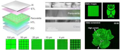
Researchers from China's Peking University, Chinese Academy of Sciences (CAS) and Southern University of Science and Technology (SUSTech) have found that the preparation of metal electrodes by high-vacuum thermal evaporation, an unavoidable step in almost all device fabrication processes, often damages the surface of perovskite films, resulting in component escape, defect density rebound, carrier extraction barrier, and film stability deterioration. Therefore, the prepared perovskite film and the final film actually working in devices are not exactly the same, and the contribution of film optimization to the device improvement is weakened. 

The team designed a bilayer structure composed of graphene oxide and graphite flakes to eliminate the unwanted film inconsistencies and thus save the film optimization loss. The team proceeded to design efficient perovskite solar cells (PSCs) with a power conversion efficiency of 25.55%, which demonstrated negligible photovoltaic performance loss after operating for 2000 hours.

Read the full story Posted: Sep 29,2024

Halocell and First Graphene enter agreement to supply graphene for perovskite solar cells

Halocell Energy has entered into an agreement with First Graphene, which will supply graphene for the manufacture of perovskite solar cells.

The initial two-year agreement will result in First Graphene providing its PureGRAPH material to Halocell for use as a high-performing coating for perovskite solar cells. By incorporating PureGRAPH into its products, Halocell Energy hopes to expedite its manufacturing process and enhance light absorbing performance, which will enable the company to scale up commercial production to meet demand.

Read the full story Posted: Sep 25,2024

Researchers design efficient carbon-based perovskite solar cells with phosphorene HTL

Researchers from Australia's Griffith University and Queensland University of Technology have reported the fabrication of planar carbon-based perovskite solar cells (c-PSCs) with high efficiency and excellent stability, by employing electrochemically produced large-area phosphorene flakes as a hole-transporting layer (HTL). 

Carbon-based perovskite solar cells have attracted increasing attention due to their many advantages, including: ease of fabrication, the potential of assembling flexible devices, low manufacturing costs and more. However, c-PSCs suffer from limited hole extraction and high charge carrier recombination due to inadequate interface contact between the carbon electrode and perovskite film.

Read the full story Posted: Jun 12,2024

Researchers examine a perovskite-graphene device for X-ray detection

Researchers at Graphenea, University of Utah and Kairos Sensors have examined a perovskite-based graphene field effect transistor (P-GFET) device for X-ray detection.

The device architecture consisted of a commercially available GFET-S20 chip, produced by Graphenea, with a layer of methylammonium lead iodide (MAPbI3) perovskite spin coated onto the top of it. This device was exposed to the field of a molybdenum target X-ray tube with beam settings between 20 and 60 kVp (X-ray tube voltage) and 30–300 μA (X-ray tube current). Dose measurements were taken with an ion-chamber and thermo-luminescent dosimeters and used to determine the sensitivity of the device as a function of the X-ray tube voltage and current, as well as source-drain voltage.

Read the full story Posted: Nov 01,2023

Researchers report perovskite nanowires-based graphene plasmonic waveguides with low loss and low gain threshold

Researchers at China's Huanghe Science and Technology University, Zhengzhou Normal University and Zhongke Weike Technology (Henan) Co., Ltd have designed a perovskite nanowire-based graphene plasmonic waveguide, where the perovskite nanowire is located on the graphene-insulator-metal (GIM) platform. The findings of this work could have potential applications in plasmonic waveguide-based devices, such as lasers, modulators, sensors, etc.

The finite element method was used in order to investigate the impact of the perovskite nanowire radius, graphene layer thickness, Fermi energy level of the graphene, thickness of the low index dielectric layer, and permittivity of dielectric layer on the mode properties. The results indicate that the hybrid mode exhibits very low propagating loss and ultra-high figure of merit. 

Read the full story Posted: Oct 23,2023

First Graphene, Halocell and QUT secure funding for perovskite PV project

Graphitic materials supplier First Graphene has announced an R&D collaboration with Greatcell Energy, trading as Halocell Energy, and the Queensland University of Technology (QUT) to commercialize perovskite solar cell fabrication. The project has received a Cooperative Research Centers Project (CRC-P) grant worth over AUD$2 million (around $USD1,300,000).

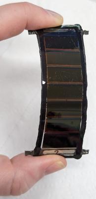
The research and development project is intended to commercialize ultra-low-cost, flexible perovskite solar cell fabrication using Halocell’s roll-to-roll production process at the company’s Wagga Wagga plant, First Graphene said in an announcement. Through the project, First Graphene plans to develop cost-effective graphene-based electrode replacements for high-cost conductor materials, such as gold and silver, used in cell manufacturing.

Read the full story Posted: Sep 04,2023

Greatcell Australia and First Graphene explore graphene enhancements to perovskite solar cells

It was recently reported that Greatcell Australia is working with graphene company First Graphene on graphene enhancements to perovskite solar cell technology.

Greatcell Australia has reportedly established a pilot plant in New South Wales and is in the advanced stages of testing its range of perovskite solar cells (PSCs) with manufacturers around the world. “Greatcell is aiming to modularize their production lines for product flexibility, due in part to the easier assembly and reduced number of steps to produce PSCs compared to silicon solar cells.”

Read the full story Posted: Apr 04,2023

Researchers present new method for fabricating thin films of perovskite oxide semiconductors

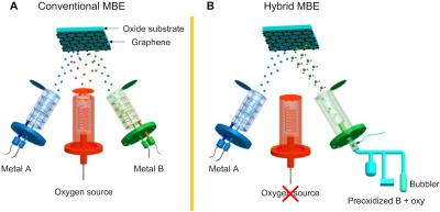
Researchers from the University of Minnesota Twin Cities-led, University of Wisconsin–Madison and Pacific Northwest National Laboratory have developed a new method for making thin films of perovskite oxide semiconductors, a class of “smart” materials with unique properties that can change in response to stimuli like light, magnetic fields, or electric fields. 

Their work could allow researchers to harness these properties and even combine them with other emerging nano-scale materials to make better devices such as sensors, smart textiles, and flexible electronics.

Read the full story Posted: Jan 04,2023

Researchers examine how molybdenum ditelluride could increase carrier generation in perovskite solar cells

Researchers from South Korea's Sungkyunkwan University (SKKU) have found that molybdenum ditelluride could increase carrier generation in perovskite solar cells.

They simulated a tandem solar cell with two absorbers based on methylammonium lead triiodide (CH3NH3PbI3) – a perovskite with high photoluminescence quantum yield – and molybdenum ditelluride (MoTe2), which is known for being naturally p-doped, with cascaded bandgaps to absorb a wider solar spectrum. The team determined that its efficiency could exceed 20%.

Read the full story Posted: Dec 06,2022

Researchers design graphene oxide/silicon heterojunction solar cell with 18.8% efficiency

Researchers from Hebei University, Karlsruhe Institute of Technology and Chinese module manufacturer Yingli Green Energy Holding Co. Ltd. have reported a heterojunction solar cell based on graphene-oxide (GO) and silicon with a large area of 5.5 cm2.

GO is a compound of carbon, oxygen and hydrogen that is obtained by treating graphite with oxidizers and acids. It consists of a single-layer sheet of graphite oxide that is commonly used to produce graphene-related nanomaterials for various applications, including electronics, optics, chemistry and more. The scientists developed an ink made of GO mixed with Nafion, that can be spin-coated on an n-type silicon wafer to form a high-quality passivating contact scheme. “Low interface recombination is provided by the Nafion and carrier selection by the GO,” the team explained, noting that the passivation scheme also includes an electron-selective passivation contact comprising n-doped hydrogenated amorphous silicon with an indium tin oxide (ITO) overlayer aimed at improving light trapping and reducing surface recombination.

Read the full story Posted: Jul 28,2022