Miniaturizing LEDs is crucial for creating ultra-high-resolution displays. Metal-halide perovskites show potential for efficient light emission, long-distance carrier transport, and scalable production of bright micro-LED displays. However, current thin-film perovskites face issues with uneven light emission and surface instability during lithography, making them unsuitable for micro-LED devices. There's a strong need for continuous single-crystal perovskite films with minimal grain boundaries, stable surfaces, and uniform optical properties for micro-LEDs. Yet, growing these films and integrating them into devices remains a challenge.
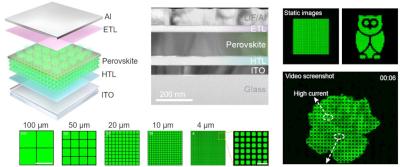
Remote epitaxial crystalline perovskites for ultrahigh resolution micro-LED displays. Image credit: Chinese Academy of Sciences
Recently, researchers from the Chinese Academy of Sciences, University of Science and Technology of China and Jilin University made significant progress in this field. The team developed a novel method for the remote epitaxial growth of continuous crystalline perovskite thin films, that allows for seamless integration into ultrahigh-resolution micro-LEDs with pixels less than 5 μm.
The results of their research describe a remote epitaxial growth technique that utilizes a graphene interlayer to create continuous crystalline perovskite thin films over an area of 4 cm2. This method effectively eliminates grain boundaries and achieves a pure out-of-plane crystallographic orientation.
Using these single-crystalline, freestanding perovskite thin films, the researchers achieved impressive results for micro-LEDs, including electroluminescence efficiency of 16.1%, brightness of 4 × 10⁵ cd m-2, and ultrahigh resolution with a pixel size of 4 μm.
The free-standing perovskites can be easily integrated with commercial electronic platforms, enabling independent and dynamic control of each pixel. This capability can be applied to both static images and video displays.
This method enables the construction of full-color micro-LED displays by integrating multiple perovskite components. Additionally, the perovskite films can be monolithically integrated with nanophotonic structures, such as resonant metasurfaces and photonic crystals, paving the way for the development of ultracompact photonic devices.


