Halide perovskite single crystals have demonstrated enormous potential for next-generation integrated optoelectronic devices. However, there is a lack of
a facile method to realize the controllable growth of large-scale, high-quality, and high-resolution perovskite single crystal arrays on diverse types of
substrates, which hinders their application in practical scenarios.
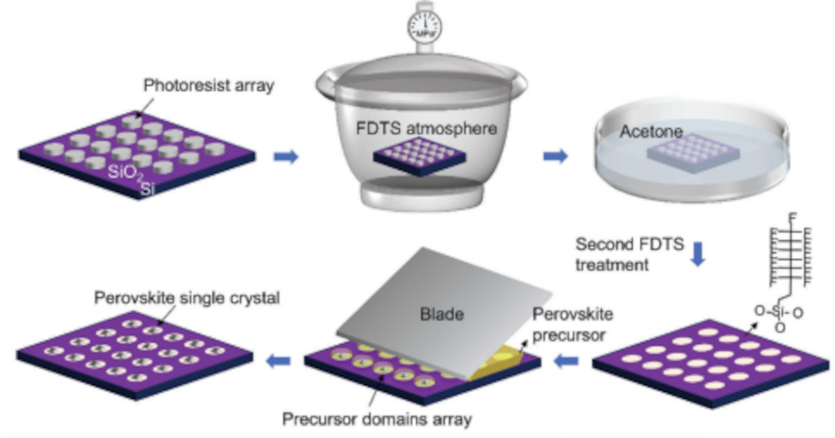
Schematic illustration of the method to prepare perovskite single crystal arrays. Image from: Advanced Science
Now, researchers from the University of Hong Kong, Nankai University and Korea Advanced Institute of Science and Technology (KAIST) have developed a one-step wettability-guided blade coating approach for the rapid in situ crystallization of large-scale, multicolor, and sub-100 nm perovskite single-crystal arrays in ambient conditions.
Using this strategy, the physical dimensions of perovskite single crystals can be precisely regulated from 90 to 260 nm, with a size variation coefficient < 10% and an area of over 900 mm2.
All three typical halogen perovskites for multi-color luminescence, CsPbX3 (X= Cl, Br, I) and their mixtures (Cl/Br or Br/I systems), are appliable for this fabrication process through the demonstration of complex RGB patterns with remarkable photoluminescence properties.
Moreover, various rigid substrates such as silicon oxide (SiO2), silicon (Si), and glass can also be used to construct the wettability-contrast templates where perovskite crystal nucleate and grow. After that, the perovskite single-crystal arrays or complex patterns can be transferred onto flexible substrates, for instance, COC.


This method combines relatively mature photolithography and low-cost solution processing to prepare large-area, high-quality perovskite single crystal arrays in a high throughput manner under ambient conditions, paving the way for integrated chips and functional optoelectronic devices.