Perovskites and graphene
Perovskites are materials that share a crystal structure similar to the mineral called perovskite, which consists of calcium titanium oxide (CaTiO3).
Depending on which atoms/molecules are used in the structure, perovskites can possess an impressive array of interesting properties including superconductivity, ferroelectricity, charge ordering, spin dependent transport and much more. Perovskites therefore hold exciting opportunities for physicists, chemists and material scientists.
Graphene is a one-atom-thick layer of carbon atoms arranged in a hexagonal lattice. It is the building-block of Graphite (which is used, among others things, in pencil tips), but graphene is a remarkable substance on its own - with a multitude of astonishing properties which repeatedly earn it the title “wonder material”. Graphene is the thinnest material known to man at one atom thick, and also incredibly strong - about 200 times stronger than steel. On top of that, graphene is an excellent conductor of heat and electricity and has interesting light absorption abilities. These varied properties make it a promising and highly researched material, with hopes of incorporating it in many applications: from inks and composite materials, through sensors, solar cells and water filters, to batteries and supercapacitors.
Due to their unique properties, carbon-based nanomaterials have been the center of extensive research efforts in various fields, one of which is the field of photovoltaic energy conversion. In recent years, hybrid metalorganic halide perovskites have become one of the most promising materials for third generation solar cells, with efficiencies that are constantly on the rise.
The incorporation of graphene into perovskite-based solar cells was naturally proposed, and significant work is taking place on this matter. Graphene-based perovskite solar cells are studied in many ways, including hole and electron transport media (HTM and ETM), electrodes, and various approaches aiming at improving the stability of the device. Tandem architectures based on graphene interlayers are also of great interest.
In addition to solar cells, other areas of graphene and perovskite integration include sensors and photodetectors, QDs, nanocatalysts and more.
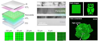
New method for remote epitaxial growth of perovskite thin films enabled high-resolution micro-LED displays
Miniaturizing LEDs is crucial for creating ultra-high-resolution displays. Metal-halide perovskites show potential for efficient light emission, long-distance carrier transport, and scalable production of bright micro-LED displays. However, current thin-film perovskites face issues with uneven light emission and surface instability during lithography, making them unsuitable for micro-LED devices. There's a strong need for continuous single-crystal perovskite films with minimal grain boundaries, stable surfaces, and uniform optical properties for micro-LEDs. Yet, growing these films and integrating them into devices remains a challenge.
Remote epitaxial crystalline perovskites for ultrahigh resolution micro-LED displays. Image credit: Chinese Academy of Sciences
Recently, researchers from the Chinese Academy of Sciences, University of Science and Technology of China and Jilin University made significant progress in this field. The team developed a novel method for the remote epitaxial growth of continuous crystalline perovskite thin films, that allows for seamless integration into ultrahigh-resolution micro-LEDs with pixels less than 5 μm.
Researchers detect and eliminate performance loss caused during the transition from perovskite films to solar cells
Researchers from China's Peking University, Chinese Academy of Sciences (CAS) and Southern University of Science and Technology (SUSTech) have found that the preparation of metal electrodes by high-vacuum thermal evaporation, an unavoidable step in almost all device fabrication processes, often damages the surface of perovskite films, resulting in component escape, defect density rebound, carrier extraction barrier, and film stability deterioration. Therefore, the prepared perovskite film and the final film actually working in devices are not exactly the same, and the contribution of film optimization to the device improvement is weakened.
The team designed a bilayer structure composed of graphene oxide and graphite flakes to eliminate the unwanted film inconsistencies and thus save the film optimization loss. The team proceeded to design efficient perovskite solar cells (PSCs) with a power conversion efficiency of 25.55%, which demonstrated negligible photovoltaic performance loss after operating for 2000 hours.
Halocell and First Graphene enter agreement to supply graphene for perovskite solar cells
Halocell Energy has entered into an agreement with First Graphene, which will supply graphene for the manufacture of perovskite solar cells.
The initial two-year agreement will result in First Graphene providing its PureGRAPH material to Halocell for use as a high-performing coating for perovskite solar cells. By incorporating PureGRAPH into its products, Halocell Energy hopes to expedite its manufacturing process and enhance light absorbing performance, which will enable the company to scale up commercial production to meet demand.
Researchers design efficient carbon-based perovskite solar cells with phosphorene HTL
Researchers from Australia's Griffith University and Queensland University of Technology have reported the fabrication of planar carbon-based perovskite solar cells (c-PSCs) with high efficiency and excellent stability, by employing electrochemically produced large-area phosphorene flakes as a hole-transporting layer (HTL).
Carbon-based perovskite solar cells have attracted increasing attention due to their many advantages, including: ease of fabrication, the potential of assembling flexible devices, low manufacturing costs and more. However, c-PSCs suffer from limited hole extraction and high charge carrier recombination due to inadequate interface contact between the carbon electrode and perovskite film.
Researchers examine a perovskite-graphene device for X-ray detection
Researchers at Graphenea, University of Utah and Kairos Sensors have examined a perovskite-based graphene field effect transistor (P-GFET) device for X-ray detection.
The device architecture consisted of a commercially available GFET-S20 chip, produced by Graphenea, with a layer of methylammonium lead iodide (MAPbI3) perovskite spin coated onto the top of it. This device was exposed to the field of a molybdenum target X-ray tube with beam settings between 20 and 60 kVp (X-ray tube voltage) and 30–300 μA (X-ray tube current). Dose measurements were taken with an ion-chamber and thermo-luminescent dosimeters and used to determine the sensitivity of the device as a function of the X-ray tube voltage and current, as well as source-drain voltage.
Researchers report perovskite nanowires-based graphene plasmonic waveguides with low loss and low gain threshold
Researchers at China's Huanghe Science and Technology University, Zhengzhou Normal University and Zhongke Weike Technology (Henan) Co., Ltd have designed a perovskite nanowire-based graphene plasmonic waveguide, where the perovskite nanowire is located on the graphene-insulator-metal (GIM) platform. The findings of this work could have potential applications in plasmonic waveguide-based devices, such as lasers, modulators, sensors, etc.
The finite element method was used in order to investigate the impact of the perovskite nanowire radius, graphene layer thickness, Fermi energy level of the graphene, thickness of the low index dielectric layer, and permittivity of dielectric layer on the mode properties. The results indicate that the hybrid mode exhibits very low propagating loss and ultra-high figure of merit.
First Graphene, Halocell and QUT secure funding for perovskite PV project
Graphitic materials supplier First Graphene has announced an R&D collaboration with Greatcell Energy, trading as Halocell Energy, and the Queensland University of Technology (QUT) to commercialize perovskite solar cell fabrication. The project has received a Cooperative Research Centers Project (CRC-P) grant worth over AUD$2 million (around $USD1,300,000).
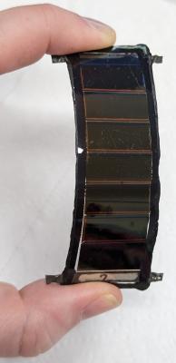
The research and development project is intended to commercialize ultra-low-cost, flexible perovskite solar cell fabrication using Halocell’s roll-to-roll production process at the company’s Wagga Wagga plant, First Graphene said in an announcement. Through the project, First Graphene plans to develop cost-effective graphene-based electrode replacements for high-cost conductor materials, such as gold and silver, used in cell manufacturing.
Greatcell Australia and First Graphene explore graphene enhancements to perovskite solar cells
It was recently reported that Greatcell Australia is working with graphene company First Graphene on graphene enhancements to perovskite solar cell technology.
Greatcell Australia has reportedly established a pilot plant in New South Wales and is in the advanced stages of testing its range of perovskite solar cells (PSCs) with manufacturers around the world. “Greatcell is aiming to modularize their production lines for product flexibility, due in part to the easier assembly and reduced number of steps to produce PSCs compared to silicon solar cells.”
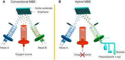
Researchers present new method for fabricating thin films of perovskite oxide semiconductors
Researchers from the University of Minnesota Twin Cities-led, University of Wisconsin–Madison and Pacific Northwest National Laboratory have developed a new method for making thin films of perovskite oxide semiconductors, a class of “smart” materials with unique properties that can change in response to stimuli like light, magnetic fields, or electric fields.
Their work could allow researchers to harness these properties and even combine them with other emerging nano-scale materials to make better devices such as sensors, smart textiles, and flexible electronics.
Researchers examine how molybdenum ditelluride could increase carrier generation in perovskite solar cells
Researchers from South Korea's Sungkyunkwan University (SKKU) have found that molybdenum ditelluride could increase carrier generation in perovskite solar cells.
They simulated a tandem solar cell with two absorbers based on methylammonium lead triiodide (CH3NH3PbI3) – a perovskite with high photoluminescence quantum yield – and molybdenum ditelluride (MoTe2), which is known for being naturally p-doped, with cascaded bandgaps to absorb a wider solar spectrum. The team determined that its efficiency could exceed 20%.
Pagination
- Page 1
- Next page


