Researchers at North Carolina State University and Brookhaven National Laboratory have reported a technique for engineering layered hybrid perovskites (LHPs) down to the atomic level, which enables precise control on how the materials convert electrical charge into light.
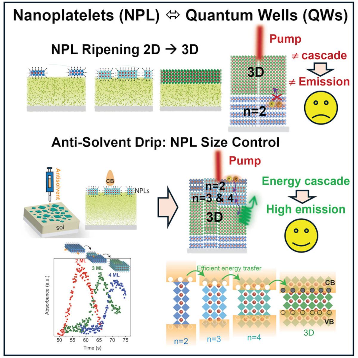
Image credit: Matter
The technique opens the door to engineering materials tailored for use in next-generation printed LEDs, lasers and photovoltaic devices.
LHPs consist of thin sheets of perovskite semiconductor material that are separated from each other by thin organic “spacer” layers. LHPs can be laid down as thin films consisting of multiple sheets of perovskite and organic spacer layers. These materials are desirable because they can efficiently convert electrical charge into light, making them promising for use in next-generation LEDs, lasers and photonic integrated circuits.
However, while LHPs have been of interest to the research community for years, there was little understanding of how to engineer these materials in order to control their performance characteristics.
Quantum wells, which are sheets of semiconductor material sandwiched between spacer layers, are an important concept to understand in the context of this recent work. “We knew quantum wells were forming in LHPs – they’re the layers,” says Aram Amassian, corresponding author of a paper on the work and a professor of materials science and engineering at North Carolina State University.


Understanding the size distribution of quantum wells is important because energy flows from high-energy structures to low-energy structures at the molecular level. “A quantum well that is two atoms thick has higher energy than a quantum well that is five atoms thick,” says Kenan Gundogdu, co-author of the paper and a professor of physics at NC State. “And in order to get energy to flow efficiently, you want to have quantum wells that are three and four atoms thick between the quantum wells that are two and five atoms thick. You basically want to have a gradual slope that the energy can cascade down.”
“But people studying LHPs kept running into an anomaly: the size distribution of quantum wells in an LHP sample that could be detected via X-ray diffraction would be different than the size distribution of quantum wells that could be detected using optical spectroscopy,” Amassian says. “For example, diffraction might tell you that your quantum wells are two atoms thick, as well as there being a three-dimensional bulk crystal". “But spectroscopy might tell you that you have quantum wells that are two atoms, three atoms, and four atoms thick, as well as the 3D bulk phase. So, the first question we had was: why are we seeing this fundamental disconnect between X-ray diffraction and optical spectroscopy? And our second question was: how can we control the size and distribution of quantum wells in LHPs?”
Through a series of experiments the researchers discovered that there was a key player involved in answering both questions: nanoplatelets.
“Nanoplatelets are individual sheets of the perovskite material that form on the surface of the solution we use to create LHPs,” Amassian says. “We found that these nanoplatelets essentially serve as templates for layered materials that form under them. So, if the nanoplatelet is two atoms thick, the LHP beneath it forms as a series of two-atom-thick quantum wells. However, the nanoplatelets themselves aren’t stable, like the rest of the LHP material. Instead, the thickness of nanoplatelets keeps growing, adding new layers of atoms over time. So, when the nanoplatelet is three atoms thick, it forms three-atom quantum wells, and so on. And, eventually, the nanoplatelet grows so thick that it becomes a three-dimensional crystal.”
This finding also resolved the longstanding anomaly about why X-ray diffraction and optical spectroscopy were providing different results. Diffraction detects the stacking of sheets and therefore does not detect nanoplatelets, whereas optical spectroscopy detects isolated sheets.
“What’s exciting is that we found we can essentially stop the growth of nanoplatelets in a controlled way, essentially tuning the size and distribution of quantum wells in LHP films,” Amassian says. “And by controlling the size and arrangement of the quantum wells, we can achieve excellent energy cascades – which means the material is highly efficient and fast at funneling charges and energy for the purposes of laser and LED applications.”
When the researchers found that nanoplatelets played such a critical role in the formation of perovskite layers in LHPs, they decided to see if nanoplatelets could be used to engineer the structure and properties of other perovskite materials – such as the perovskites used to convert light into electricity in solar cells and other photovoltaic technologies.
“We found that the nanoplatelets play a similar role in other perovskite materials and can be used to engineer those materials to enhance the desired structure, improving their photovoltaic performance and stability,” says Milad Abolhasani, co-author of the paper and ALCOA Professor of Chemical and Biomolecular Engineering at NC State.