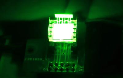
A team of researchers, led by Professor David Di from the International College of Zhejiang University and the School of Optoelectronic Science and Engineering, recently achieved a continuous transition from n-type to p-type perovskite semiconductors through molecular doping, while maintaining extremely high luminescence performance.
Image credit: Zhejiang University
Based on controllable doping, the team developed a perovskite LED with a simple structure and reported a record for the highest brightness of solution-based LEDs, reaching 1.16 million nits.
A key reason why semiconductor materials are so widely used in electronic technology is that they can achieve two different conductive properties, p-type and n-type, through doping. For traditional semiconductors, effective control of their electrical properties can be achieved through "doping", that is, introducing impurities into the crystal lattice. For example, doping silicon with boron can make it a p-type semiconductor that mainly conducts positive charges (holes), while doping with phosphorus can make it an n-type semiconductor that mainly conducts negative charges (electrons). The pn junction formed between p-type and n-type semiconductors is the basis of modern electronic technology.
At the pn junction interface, electrons and holes recombine to generate a current that changes dramatically with voltage, thereby achieving basic functions such as rectification, amplification, and switching, which are then applied in various electronic devices. The regulation of semiconductor electrical properties has led to revolutionary inventions including diodes, transistors, solar cells, detectors, LEDs, and semiconductor lasers.
In perovskite halides, due to their complex structure and composition, it is challenging to achieve precise control of the electrical properties. Previous studies have tried a variety of methods, but it is difficult to achieve good electrical control while maintaining high luminous efficiency.
"As a member of the semiconductor family, perovskite should be able to adjust the polarity and concentration of carriers by doping, just like other semiconductor materials," said David Di. "A series of experiments we conducted also confirmed this: after the introduction of doping, the Fermi level of perovskite (that is, the expected energy of electrons) gradually moved from the high-energy side of the semiconductor band gap to the low-energy side. This means that perovskite can achieve a transition from n-type, which is conducive to the conduction of electrons (negative charges), to p-type, which is conducive to the conduction of holes (positive charges). "
The dopant used by the team, 4PACz, has been widely used as an ultra-thin molecular layer material for high-efficiency perovskite solar cells in the past. Zhao Baodan said: "We accidentally discovered that 4PACz, a very common material in the laboratory, has a strong electron-withdrawing ability. When introduced into perovskite semiconductors as a dopant, it can effectively transform the originally n-type perovskite into p-type. At the same time, after the introduction of doping, the perovskite semiconductor still maintains a high fluorescence efficiency. In addition, we have also discovered an n-type dopant suitable for perovskite."
Effectively controlling the electrical properties of perovskite semiconductors could pave the way towards the design and manufacture of various electronic devices. Typically, perovskite LEDs contain both an electron transport layer and a hole transport layer to achieve efficient carrier injection, thereby ensuring excellent device performance. The simplified perovskite LED structure without a hole transport layer has the advantages of low preparation cost and high reproducibility, but usually has low luminous efficiency.
Image
In their recent work, through controllable doping technology, the research team successfully prepared a perovskite LED with excellent performance without a hole transport layer. At the same time, it also shows great advantages over conventional LEDs.
"Surprisingly, the p-type perovskite LED prepared by introducing 4PACz doping not only has a simple structure, but also achieves a maximum brightness of 1.16 million cd/m2 (1.16 million nits), as well as an external quantum efficiency of 28.4% and an energy conversion efficiency of 23.1%." Xiong Wentao said, "The ultra-high brightness of these devices has refreshed the record of solution-processed LEDs (including OLEDs, quantum dot LEDs and perovskite LEDs), and its energy conversion efficiency is the highest level of visible light perovskite LEDs."
Furthermore, the team explored the working principles of these high-performance perovskite LEDs through device modeling and optical measurements. The results are highly consistent with their previous understanding that the changes in p-type conduction behavior and carrier recombination zone caused by doping are the main contributing factors to the excellent performance of these hole-transport layer-free devices.
"The ability to control the polarity and concentration of carriers in perovskite semiconductors means the possibility of new device design and functional development. The high-brightness perovskite LEDs and pn junction diodes we developed are just some preliminary demonstrations. Controllably doped perovskite semiconductors are expected to bring about a new generation of optoelectronic devices," said David Di.


