New JV by Voltec and IPVF called "France PV Industrie" to establish 5 GW factory for 4T tandem perovskite-silicon modules

French solar module manufacturer Voltec Solar and the Institut Photovoltaïque d’Île-de-France (IPVF) have announced plans to set up a factory for four-terminal (4T) tandem perovskite-silicon solar panels in France. The “France PV Industrie” project aims to build a gigafactory for solar panels, with a dual objective: to produce more efficient solar panels locally and to create a sustainable industry, based on a fast-growing market and a breakthrough technology.

The IPVF and Voltec plan to create a joint venture (France PV Industrie) so they can secure the necessary financing to scale up to industrial production. The pilot line will require an investment of €15 million ($15.4 million) and the industrial demonstrator €50 million. The partners estimate the total investment at around €1 billion by 2030. The facility will make modules based on IPVF's 4T tandem solar cell technology. The two entities plan to set up the first pilot production line by the end of 2023 and the first 200 MW industrial demonstrator in 2025. They will then increase the factory's capacity to 1 GW in 2027 and 5 GW by 2030.

Read the full story Posted: Nov 15,2022

Researchers demonstrate perovskite phase heterojunction (PHJ) solar cells

Researchers from the Technical University of Dresden, led by Prof. Yana Vaynzof, have demonstrated a new concept for the formation of a heterojunction for photovoltaics. The team took advantage of the fact that materials can often exist in different structural configurations, termed crystalline phases. This phenomenon, called polymorphism, means that the same material can exhibit different properties, depending on the specific arrangements of atoms and molecules in its structure.

By interfacing two such phases of the same material, Prof Vaynzof and her team demonstrated for the first time the formation of a phase heterojunction solar cells. Specifically, the researchers chose a caesium lead iodide perovskite – a highly efficient solar cell absorber material – in the beta and gamma phases to realise their new concept.

Read the full story Posted: Nov 12,2022

Researchers develop bright, efficient and stable perovskite light-emitting diodes

Researchers from Korea's PEROLED, Seoul National University and Korea Basic Science Institute (KBSI), along with scientists from the UK's University of Cambridge, have reported an ultra-bright, efficient and stable perovskite LED made of core/shell perovskite nanocrystals with a size of approximately 10 nm, obtained using a simple in situ reaction of benzylphosphonic acid (BPA) additive with three-dimensional (3D) polycrystalline perovskite films, without separate synthesis processes.

During the reaction, large 3D crystals are split into nanocrystals and the BPA surrounds the nanocrystals, achieving strong carrier confinement. The BPA shell passivates the undercoordinated lead atoms by forming covalent bonds, and thereby greatly reduces the trap density while maintaining good charge-transport properties for the 3D perovskites.

Read the full story Posted: Nov 11,2022

Researchers from the University of Japan develop a perovskite-based narrow-spectrum blue QD emitter

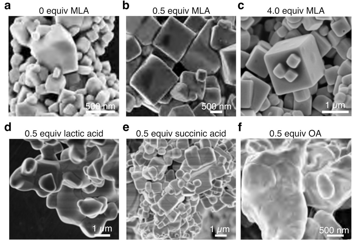
Researchers from the University of Tokyo have made progress with the development of blue-emitting quantum dots, which is seen as highly challenging. They have shown that using a new bottom-up design strategy and self-organizing chemistry can help create a high purity blue-emitting QD material (with a narrow emission spectrum).

Electric Microscope images of experimental QDs, University of Tokyo


The newly developed QDs have a special chemical composition that combines both organic and inorganic substances, such as lead perovskite, malic acid, and oleylamine. The materials self-aligned into a cube of 64 lead atoms. The lead researcher, Professor Eiichi Nakamura, says that "it took over a year of methodically trying different things to find that malic acid was a key piece of our chemical puzzle".

Read the full story Posted: Nov 11,2022

CATL reveals patents for perovskite-based PV products

It was recently reported that Contemporary Amperex Technology Limited (CATL), the Chinese manufacturer of energy devices, has filed to publicize its patents for the designs and manufacturing processes of several PV products.

The patents, which have been applied under the category of solar PV products, cover a backsheet, a transparent substrate, a perovskite PV cell, and a device design.

Read the full story Posted: Nov 10,2022

Perovskite panchromatic absorber could improve photoelectrochemical cell for hydrogen production

Researchers from Ulsan National Institute of Science and Technology (UNIST) have designed a photoelectrochemical cell for hydrogen production utilizing a high-performance organic–inorganic halide perovskite as a panchromatic absorber. The cell achieved a record high photocurrent density of 19.8 mA cm−2.

Solar hydrogen production is one of the ultimate technologies needed to realize a carbon-neutral, sustainable society. However, an energy-intensive water oxidation half-reaction together with the poor performance of conventional inorganic photocatalysts have been big hurdles for practical solar hydrogen production. This study paves the way to improve solar hydrogen productivity.

Read the full story Posted: Nov 08,2022

Researchers use surface modulators to achieve efficient inverted perovskite solar cells

Researchers from the University of Surrey, Swansea University, University of Sheffield, University of Cambridge and University of Oxford in the UK, China-based CAS and Canada's University of Toronto have fabricated an inverted perovskite solar cell by using a surface modulator that reportedly facilitates superior passivation on perovskite surfaces, increasing overall cell efficiency. As the surface modulator, the scientists tested two organic halide salts known as 4-hydroxyphenethylammonium iodide (HO-PEAI), and 2-thiopheneethylammonium iodide (2-TEAI).

“These modulators can affect the surface energy of the perovskite films,” the team explained. They explained that the two compounds can dramatically reduce non-radiative interfacial recombination. This can have a significant impact on electrical performance in perovskite cells, with implications for open-circuit voltage, short-circuit current, fill factor, and ultimately, power conversion efficiency. They reported that “2-TEAI showed a stronger interaction than HO-PEAI, forming a quasi-2D structure on the perovskite surface without further annealing.”

Read the full story Posted: Nov 07,2022

Researchers use Sulfonium cations to improve quasi-2D perovskite solar cells

Researchers from the National Center for Nanoscience and Technology (NCSNT) of the Chinese Academy of Sciences (CAS) and Beihang University have developed a sulfonium cations-assisted intermediate engineering strategy to study the evolution of intermediates and the film properties of quasi-2D perovskites. The researchers developed a facile strategy for intermediate engineering by employing sulfonium cations to regulate the transformation of intermediates during the crystallization process and improve the film quality of quasi-2D perovskites.

The intermediates were characterized by X-ray diffraction (XRD) and scanning electron microscopy (SEM) to reveal the composition and transformation process of the intermediates. The introduction of sulfonium cations inhibited the formation of unfavorable solvated lead iodide and promoted the formation of favorable perovskite intermediates with fiber-like morphology, which is conducive to the formation of high-quality perovskite crystals. The above effects have been confirmed in quasi-2D perovskite with different n values and 3D perovskites.

Read the full story Posted: Nov 06,2022

Researchers develop high-resolution perovskite nanocrystal patterning technique for displays

Researchers from the Ulsan National Institute of Science and Technology (UNIST) have teamed up with researchers from Daegu Gyeongbuk Institute of Science and Technology (DGIST) to develop a patterning technique for the production of perovskite nanocrystal displays which are ultra-thin and high-resolution. The production involves a very simple stamp-like printing process that will facilitate the commercialization of the new technique.

Double-layer transfer printing process with RGB pixelated arrays of PeNCs. Image from Science Advances

The technique reportedly enabled the team to produce a display with RGB pixel patterns of 2,550 pixels per inch, which is about 400 percent higher resolution than the latest high-end smartphones.

Read the full story Posted: Nov 01,2022