Perovskite materials - Page 9

Scientists suggest new perovskite processing method

Researchers from ITMO University, the Far Eastern Federal University (FEFU), the Image Processing Systems Institute of RAS, and Tokai University (Japan) have discovered a way to fashion perovskite microcrystals into desired shapes for further use in the production of lenses and other optoelectronic elements without loss of quality.

This research opens up new opportunities for the creation of micro-optical elements that could be used in microchips and other optoelectronic devices.

Read the full story Posted: Jun 28,2021

Small-angle scattering helps reveal the colloidal nature of halide perovskite precursor solutions

Researchers at HZB, Humboldt University and Technische Universität Berlin have used small-angle scattering at the PTB X-ray beamline of BESSY II to experimentally investigate the colloidal chemistry of perovskite precursor solutions used for solar cell production. The results could contribute to the optimization of the manufacturing process and quality of perovskite materials.

Until now, the team explains, it has not been possible to achieve a comprehensive impression of the role of the colloidal chemistry in the precursor that is considered to be directional for crystallinity and the further processing. Now, a team led by Prof. Antonio Abate has used small-angle scattering to experimentally determine how the initially disordered elements in the precursor solution find their way into primary subunits, interacting and thus providing a first "pre crystalline" arrangement for further conversion to perovskite thin films.

Read the full story Posted: Jun 27,2021

Rice team grows uniform 2D perovskite crystals from seeds

Rice University scientists have created microscopic seeds for growing uniform 2D perovskite crystals that are both stable and highly efficient at harvesting electricity from sunlight. Rice's seeded growth method addresses both performance and production issues and could promote perovskite photovoltaic technology.

Chemical engineers from Rice's Brown School of Engineering describe how to make the seeds and use them to grow homogenous thin films of materials comprised of uniformly thick layers. In laboratory tests, photovoltaic devices made from the films proved both efficient and reliable, a previously problematic combination for devices made from either 3D or 2D perovskites.

Read the full story Posted: Jun 24,2021

Perovskite material superfluoresces at high temperatures

Researchers from North Carolina State University have shown that a commonly studied perovskite can superfluoresce at temperatures that are practical to achieve and at timescales long enough to make it potentially useful in quantum computing applications. The team also found that superfluorescence may be a common characteristic for this entire class of materials.

Superfluorescence is an example of quantum phase transition ' when individual atoms within a material all move through the same phases in tandem, becoming a synchronized unit.

Read the full story Posted: Jun 23,2021

Pre-synthesized perovskite material reduces defects and improves solar cell performance

researchers at the Okinawa Institute of Science and Technology Graduate University (OIST), led by Professor Yabing Qi, have demonstrated that creating a raw material used for perovskite solar cells in a different way could be key to the success of these cells.

Pre-synthesized crystalline perovskites improves PSCs image

'There's a necessary crystalline powder in perovskites called FAPbI3, which forms the perovskite's absorber layer,' explained one of the lead authors, Dr. Guoqing Tong, Postdoctoral Scholar at OIST. 'Previously, this layer was fabricated by combining two materials ' PbI2 and FAI. The reaction that takes place produces FAPbI3. But this method is far from perfect. There are often leftovers of one or both of the original materials, which can impede the efficiency of the solar cell.'

Read the full story Posted: Jun 22,2021

Researchers quantify photoinduced polaronic distortions in inorganic lead halide perovskite nanocrystals

Understanding the charge mobility of lead-halide perovskite materials is crucial for their use in photovoltaic applications. Using X-ray spectroscopic techniques, the structural deformations affecting the charge mobility, which plays a central role in solar energy conversion, have been identified and quantified by an international team of scientists led by Giulia Mancini (at the University of Pavia) and M. Chergui at EPFL.

Transport phenomena at the nanoscale image

Lead-halide perovskites' use in photovoltaic applications relies on the generation of charges (electrons and hole) upon absorption of light. These charges migrate through the material to generate an electrical current. One of the crucial physical properties in this respect is the so-called charge mobility. Despite their remarkable performances in light-to-electricity conversion, a limitation of perovskites is their charge mobilities, which are orders of magnitude smaller than those of conventional semi-conductors used in photovoltaics.

Read the full story Posted: Jun 08,2021

Sheffield researchers find that low temperatures extend lifetimes of perovskite materials

Researchers at the University of Sheffield have found that storing perovskite precursor solutions at low temperatures extends their operational lifetime from under a month to over four months.

Understanding how to make perovskite solutions more durable and reliable could potentially make the manufacture of perovskite solar cells more efficient, as the process would require fewer batches of more stable material to be produced, saving time, reducing material waste and also allowing device yield and efficiency to be optimized.

Read the full story Posted: Jun 01,2021

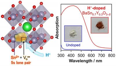
Researchers develop Sn-based perovskite material with a wide visible-light absorption band

Semiconductors that can exploit the omnipresent visible spectrum of light for different technological applications are highly sought after, but such semiconductors are often dexpensive and toxic. A group of scientists from Tokyo Institute of Technology and Kyushu University have collaborated to develop a low-cost and non-toxic narrow-gap semiconductor material with potential 'light-based' or photofunctional applications.

A cheaper perovskite-based semiconductor material that is free of toxic lead and can absorb a wide range of visible light with potential photofunctional applications image

Tin-containing oxide semiconductors are cheaper than most semiconductor materials, but their photofunctional applications are constrained by a wide optical band gap. The team of scientists, led by Dr. Kazuhiko Maeda, Associate Professor at the Department of Chemistry, Tokyo Institute of Technology, developed a perovskite-based semiconductor material that is free of toxic lead and can absorb a wide range of visible light.

Read the full story Posted: Jun 01,2021

TCI starts offering new hole selective self-assembled monolayer forming agents to boost perovskite PV performance

The following is a sponsored post by TCI

Tokyo Chemical Industry Company Limited (TCI) is now offering new hole selective self-assembled monolayer (SAM) forming agents, 2PACz [C3663], MeO-2PACz [D5798] and Me-4PACz [M3359] for high performance perovskite solar cells and OPVs.

TCI SAM materials chart, structure and image

The new materials enable efficient, versatile and stable p-i-n perovskite solar cell devices. These materials are useful for tandem solar cells as they grant conformal coverage on rough textures. In fact, a perovskite solar cell that uses the SAM hole transport layer can realize more than 20% efficiency without using dopants or additives. Perovskite-Silicon tandem solar cells that use Me-4PACz as a hole contact material realized 29.15% efficiency. Costs are lowered thanks to extremely low material consumption, and the processing is very simple and scalable.

Read the full story Posted: Jun 01,2021

Scientists propose a sandwich-like structural model for quasi-2D perovskite films

A research team, led by scientists at the ARC Centre of Excellence in Exciton Science, has shown that the two-dimensional (2D) thin films used in some perovskite solar cells closely resemble a sandwich.

This discovery changed common concepts as previously, scientists thought these 2D perovskite films had a 'gradient' structure, in which certain components were found deep in the material, with other complementary elements only located nearer to the surface. However, the members of Exciton Science based at the University of Melbourne, together with collaborators at Australia's national science agency CSIRO and Shandong University, have provided evidence for a sandwich-like structure, in which two layers of the same type (the bread) surround one central, contrasting layer (the filling).

Read the full story Posted: May 24,2021