Perovskite LED - Page 5
Researchers fabricate full-color flexible microLEDs using perovskite QDs
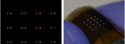
Researchers from Korea's KIMM institute have fabricated full-color flexible microLED devices, using blue LEDs and perovskite quantum dot color conversion layers. The demonstrated device featured 1 mm pixel pitch LEDs (25.4 PPI) and could be bent with a radius of 5 mm without being damaged.

The researchers used a perovskite-QD and siloxane composite using ligand exchanged PQD with silane composite followed by surface activation by an addition of halide-anion containing salt. Due to this surface activation, the researchers say that it was possible to construct the PQD surface with a silane ligand using a non-polar organic solvent that does not damage the PQD. As a result, the ligand-exchanged PQD with a silane compound exhibited high dispersibility in the siloxane matrix and excellent atmospheric stability.
Researchers report molecular engineering strategy for efficient and stable deep-red perovskite LEDs
Researchers from Purdue University, Florida State University, University of Kentucky, Lawrence Berkeley National Laboratory, University of Houston, Rice University, China's Qilu University of Technology (Shandong Academy of Sciences) and Taiwan's National Cheng Kung University have found that LEDs based on halide perovskites can produce more vivid, colorful and brighter images. The recent research presents extremely efficient perovskite LED devices in the red color region.
Perovskite materials often tend to be less stable and can degrade quickly. Further, device efficiency has not been fully optimized to compete with conventional LEDs. “Our work aims to resolve these critical issues,” said Purdue's Letian Dou, who conceived the idea, supervised the project and provided funding support.
Researchers improve perovskite-based LEDs using self-assembled molecules
Researchers from the Institute of Chemical Research of Catalonia-The Barcelona Institute of Science and Technology (ICIQ-BIST), Centre Tecnològic de Catalunya EURECAT, Istituto Italiano di Tecnologia (IIT), ICREA and Universitat Rovira i Virgili have reported the application of two carbazole-based self-assembled molecules (SAMs) as hole injecting materials in perovskite-based LEDs.
Their structures differ in one phenyl ring in the bridge; however, the extra ring provides more stability to the devices, even surpassing the one obtained with the widely used polymer PTAA. In addition, due to the structural and electronic characteristics of the SAMs, the efficiency of the devices is also increased.
Researchers report on novel approach for high performance and spectrally stable deep-blue perovskite LEDs
Researchers from Yonsei University, Sungkyunkwan University and Institute for Basic Science (IBS) have proposed a rapid crystallization method based on hot-antisolvent bathing for realization of deep-blue perovskite light-emitting diodes (PeLEDs). The rapid crystallization method manipulates 2D perovskite phase evolution by controlling the crystallization kinetics for the fabrication of phase-pure 2D Ruddlesden‒Popper perovskites (2D-RPPs), enabling deep-blue-emissive perovskite LEDs.
PeLEDs are considered as promising candidates for next-generation solution-processed full-color displays. However, the external quantum efficiencies (EQEs) and operational stabilities of deep-blue (<460 nm) PeLEDs still lag far behind their red and green counterparts. 2D-RPPs have excellent optoelectronic properties—ideal for LEDs. Although 2D-RPP-based LEDs have rapidly progressed in terms of performance, it is still challenging to demonstrate blue-emissive and color-pure LEDs. The deep blue of current LED displays is usually produced by indium gallium nitride (InGaN), a costly substance. In the field of LEDs, researchers are seeking alternatives and one of them could be found in 2D-RPPs.
Researchers achieve single component white LEDs based on lanthanide ions doped lead halide perovskite
Researchers from China's Jilin University have developed a promising method to fabricate white perovskite LEDs using lanthanides (Ln3+) ions doped CsPbCl3 perovskite nanocrystals (PeNCs).
Lead halide perovskite nanocrystals (PeNCs) have attracted extensive attention due to their high photoluminescence quantum yield (PLQY), adjustable bandgap, low cost, and excellent photoelectric properties. In recent years, perovskite based light emitting diodes (LEDs) have developed rapidly and become candidates for low-cost, solution-processing based solid-state lighting. White light perovskite LEDs are possible to be obtained by stacking different NCs with complementary emissions together in one film. However, the halide ion segregation and exchange lead to severe color instability and complex structure in mixed halide perovskite LED devices. Therefore, new technologies are required for the development of white light devices.
The MicroLED Industry Association to host a Perovskite microLED technology webinar
On March 27 the MicroLED Industry Association will host a private webinar on perovskite materials for the microLED industry. Perovskite materials hold great promise for the solar industry and in recent years we are seeing promising signs for the adoption of perovskites the display industry.

The upcoming Seminar will feature four world-leading speakers, and will also be open to a Q&A session. We will learn more about the state-of-the-art perovskite research and development, with a focus of course on applications in the microLED industry - for both perovskite QDs and PeLEDs.
Researchers develop bright, efficient and stable perovskite light-emitting diodes
Researchers from Korea's PEROLED, Seoul National University and Korea Basic Science Institute (KBSI), along with scientists from the UK's University of Cambridge, have reported an ultra-bright, efficient and stable perovskite LED made of core/shell perovskite nanocrystals with a size of approximately 10 nm, obtained using a simple in situ reaction of benzylphosphonic acid (BPA) additive with three-dimensional (3D) polycrystalline perovskite films, without separate synthesis processes.
During the reaction, large 3D crystals are split into nanocrystals and the BPA surrounds the nanocrystals, achieving strong carrier confinement. The BPA shell passivates the undercoordinated lead atoms by forming covalent bonds, and thereby greatly reduces the trap density while maintaining good charge-transport properties for the 3D perovskites.
Researchers develop high-resolution perovskite nanocrystal patterning technique for displays
Researchers from the Ulsan National Institute of Science and Technology (UNIST) have teamed up with researchers from Daegu Gyeongbuk Institute of Science and Technology (DGIST) to develop a patterning technique for the production of perovskite nanocrystal displays which are ultra-thin and high-resolution. The production involves a very simple stamp-like printing process that will facilitate the commercialization of the new technique.
Double-layer transfer printing process with RGB pixelated arrays of PeNCs. Image from Science Advances
The technique reportedly enabled the team to produce a display with RGB pixel patterns of 2,550 pixels per inch, which is about 400 percent higher resolution than the latest high-end smartphones.
Researchers utilize nano-optical designs for high-efficiency perovskite–silicon tandem solar cells
Researchers from Helmholtz-Zentrum Berlin (HZB) and Potsdam University have reported perovskite–silicon tandem solar cells with periodic nanotextures that offer various advantages without compromising the material quality of solution-processed perovskite layers. Textured tandem devices have been presented before, aiming at improved optical performance, but optimizing film growth on surface-textured wafers has thus far remained challenging.
The research team showed a reduction in reflection losses in comparison to planar tandems, with the new devices being less sensitive to deviations from optimum layer thicknesses. The nanotextures also enabled a greatly increased fabrication yield from 50% to 95%. Moreover, the open-circuit voltage was improved by 15 mV due to the enhanced optoelectronic properties of the perovskite top cell. The optically advanced rear reflector with a dielectric buffer layer resulted in reduced parasitic absorption at near-infrared wavelengths. As a result, the team achieved a certified power conversion efficiency of 29.80%.
The Perovskite for Displays Market Report updated to September 2022
Perovskite-Info is proud to announce an update to our Perovskite for the Display Industry Market Report. This market report, brought to you by the world's leading perovskite and OLED industry experts, is a comprehensive guide to next-generation perovskite-based solutions for the display industry that enable efficient, low cost and high-quality display devices. The report is now updated to September 2022, with all the latest commercial and research activity.
Reading this report, you'll learn all about:
- Perovskite materials and their properties
- Perovskite applications in the display industry
- Perovskite QDs for color conversion
- Prominent perovskite display related research activities
The report also provides a list of perovskite display companies, datasheets and brochures of pQD film solutions, an introduction to perovskite materials and processes, an introduction to emerging display technologies and more.
Pagination
- Previous page
- Page 5
- Next page


